
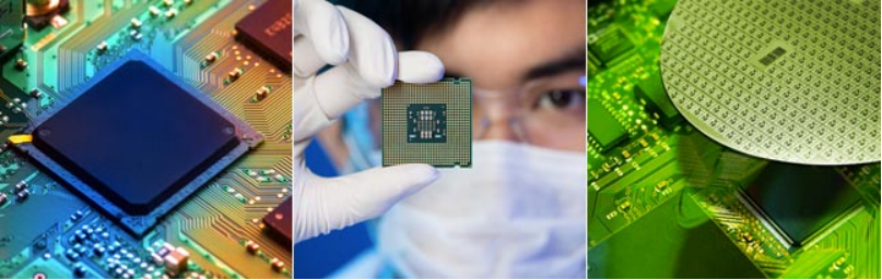
Application of semiconductor industry with machine vision lighting
The application of semiconductor industry with machine vision lighting began as early as 20 years ago. semiconductor and electronic equipment not only is the birthplace of machine vision technology, but also has been one of the huge markets for machine vision. As you know, the semiconductor and manufacturing of electronics will keep upgrade for the future such as: The wafer is getting bigger and the wir3es inside are getting thinner, get using on more and more ultra-fine components devices. The size of the connector is getting smaller and smaller, and the number of testing and measuring devices on the production line is increasing every minute, which will be accompanied by the birth of a new round of semiconductor and electronic production equipment. It will produce a new quality assurance system to improve its productivity and ensure zero defect rate, then promote market of the machine vision continues to grow up. Machine vision technology will also has been improved and developed with the development of semiconductor, electronics, optics, automation and other technologies.
What are the applications of machine vision in semiconductors? Let our visual engineer from out company LOTS which have rich experience in this business, will introduce to you, which kind of new technology breakthroughs in semiconductors need to use by the machine vision.
※Surface recognition/controllability test
※Measurement /Mark point
※Classification
Surface recognition /controllability test
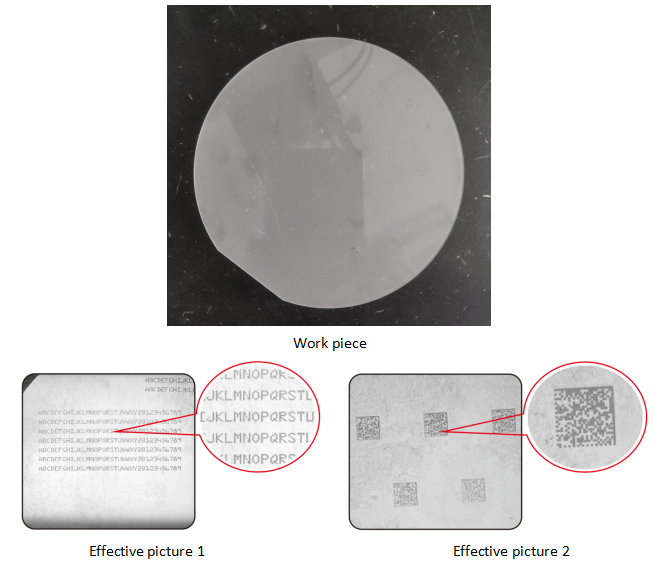
In the semiconductor industry, to maintain the controllability of the product, all components have recognition codes, and you can get the information on recognition codes also the judgments can be made. So the semiconductor surface printing, ID code, QR code, mark point and so on, get full use of the machine vision lighting.
As for the higher accuracy product and which has more recognition details on the surface, less tolerance for defects in the component itself. Therefore, judgment of surface defect also makes machine vision became important in the industry.
Wafer printing recognition
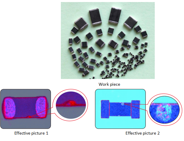
Measurement /Mark point
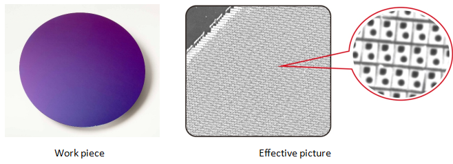
Mark point plays an important role in the whole wafer process. because measurement/mark point are wrong can be damage many wafer, so a bad vision system can increase a lot of costs of a semiconductor equipment company, also will affect the vision system's effective picture.
LOTS has an professional team to give you the best solution to inspect the wafers on the semiconductor,it will help you to avoid the problem of a wrong measurement/mark point from effect of the visual system imaging. we have many experience in the semiconductor industry and make sure the equipment performance throughout the semiconductor manufacturing process.
Mark point on wafer
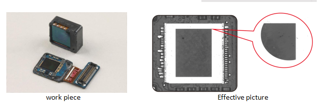
Measurement the chip of the camera
Classification
In the semiconductor industry classification many scenes will be used, semiconductor in the manufacturing process has high requirement, not only high-speed, efficient, to make sure that every step needs to be very careful. Machine vision can get full use in semiconductors industr because accurate manufacturing process. For example: defect classification, positive and negative screening, uncontrollable grasp recognition and etc.
Those process technology can greatly improve the accuracy of machine vision system, so the choice of machine vision light is important. Although LOTS (Lighting & Tech Specialist Optics) is a machine vision light manufacturer. But it has made great contributions to machine vision. We have many years cooperation with semiconductor, new energy, medical, automotive, military and other equipment system integrators. For different projects, the selection of light source, camera, lens and other hardware for each equipment intelligent manufacturers to solve the problems.


 Ms.Cici
 8618319014500